We design boards using PADS Layout and Altium and schematics using PADS Logic, Altium and OrCAD Capture.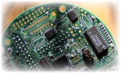
Our schematics are designed to be easily understood and legible at 8 x 11″.
Our boards are always designed for manufacturability with careful attention to placement, even at the prototype stage. We recommend designing for test, with 100% access, and can add ICT points at the customer’s discretion.
All of our boards are hand routed unless explicitly requested by the customer. This policy ensures the most direct connectivity, the greatest reliability and the highest yield.
We are in business for service. With that in mind, our boards are turned very professionally and quickly.
Our experience includes but is not limited to:
- Schematic Capture
- Prototype and Production Boards
- Design for Manufacturability
- Design for Test
- Analog/Digital Design
- RF Design
- Hand Routing
- MIL Spec
- LTCC Multi-Chip Module
- Multi-Layer
- Multi-Sided
- ICT
- BGA
- Flex
- 3D files in Altium and PADS